The first in a series of posts for researchers on how to emulate, debug and fuzz UEFI modules, we begin with a refresher on how to dump SPI flash memory.
By Assaf Carlsbad and Itai Liba
Introduction
At the time of writing, the UEFI specification has already reached version 2.8. Being a nearly 20-year old standard (the now deprecated version 1.1 of the specification was released in late 2002), it’s a safe bet to assume that most folks working in the information security industry have heard the term UEFI at least once during their career. A slightly more daring, but still relatively safe, bet is to put one’s money on the assertion that in addition to merely knowing about its existence, most security professionals also have some vague idea about what UEFI is and what it tries to accomplish. In a quick and not-so-scientific poll we conducted with the help of some of our colleagues, most of them knew that UEFI deals with firmware, that it is essentially a replacement for the legacy BIOS from the joyful IBM PC days and that it serves as a foundation on top of which several security-related features, such as Secure Boot, can be implemented.
However, when asked how many of them have actual, hands-on experience with UEFI, the number of pointing fingers raised into the air dropped dramatically. There’s actually a pretty good reason for that: firmware security in general and UEFI security in particular are still considered niche topics, way outside of mainstream popularity. In recent years, things have been getting much better on that front, with websites, books and even training classes dedicated almost entirely to the subject. But still, the amount of attention firmware security gets is just a tiny fraction compared to what other, more accessible domains such as network security or OS security usually get from the community. Thus, it should come as no surprise that the average security researcher has never peeked into the UEFI firmware on his or her machine and has never attempted to reverse engineer it, let alone fuzz it.
Albeit understandable, the current state of things is still pretty far from optimal. The reason for that is twofold. First of all, UEFI is ubiquitous. It is ubiquitous in the sense that a UEFI compliant firmware can be found almost everywhere, starting from low-end Raspberry PI SOCs going through all mainstream laptops and desktop computers and ending up with ultra high-end servers. The second reason for the importance of UEFI security has to do with the tier-like nature of modern computer architecture, in which every layer of the stack is only as secure as the layer below it. Since the firmware “sits” really close to the bottom of this stack (usually right above the hardware), a firmware-level threat has the potential to compromise the security of an entire system, while bypassing many traditional kernel-based or even hypervisor-based mitigations.
This blog post is the first in a series of posts in which we’ll try to shed some light on the subject with the declared aim of helping more researchers in the community get onboard the UEFI “train”. In this post, we’ll mainly focus on providing the theoretical background as well as the practical knowledge required in order to acquire a dump of the UEFI firmware, often found on the SPI chip. Future posts will pick up where this post concludes and will discuss methods to reverse, debug, and fuzz individual UEFI drivers. Although the ride isn’t particularly cosy and can get bumpy at times, we believe that the view as seen from the top of the “UEFI mountain” is well worth the journey.
SPI Flash & PCI devices
Before any reversing or fuzzing can take place, we first need to figure out where the UEFI firmware is stored and how we can acquire it, i.e. dump an offline version of it to disk for further analysis. To the best of our judgement, it’s almost impossible to describe this procedure without referring to this excellent whitepaper by ESET on a piece of malware called LoJax. In a nutshell, LoJax was a bootkit which – up to and during 2018 – managed to exploit a certain hardware misconfiguration as a means to infect the victim’s UEFI firmware. Because of the low-level nature of the infection, LoJax had a rather unique degree of persistence: it could survive OS reinstallation, hard-drive replacement, and most other techniques IT personnel typically use to clean infected machines.
To be able to perform the infection, LoJax first had to dump the contents of the UEFI firmware, patch it with its malicious payload, and then flash it back. Based on this description, it is quite clear that we can acquire our own firmware simply by following the path LoJax delineated for us. Below is the relevant excerpt from section 4 of the whitepaper, outlining the process:
“The tool’s … task is to retrieve the BIOS region base address on the SPI flash memory as well as its size. This information is contained in the SPI Host Interface register “BIOS Flash Primary Region”. All SPI Host Interface registers are memory-mapped in the Root Complex Register Block (RCRB) whose base address can be retrieved by reading the correct PCI Configuration Register. ReWriter_read obtains this address by using RwDrv IOCTL 0x22840 and reading the correct offset (0xF0 in our case). Once the BIOS region base address and size are known, the dump tool reads the relevant content of the SPI flash memory and writes it to a file on disk.”
Unfortunately, this paragraph doesn’t make a lot of sense to someone who isn’t already familiar with some of the terminology and acronyms prevalent in the UEFI world. Therefore, to make things easier on our digestive system, we should dedicate the next few sections to breaking it apart, de-mystifying the terms, and making sure the process is well established. We will give special attention to the SPI flash memory as well as to some aspects of the PCI standard.
The SPI Flash Memory
The Serial Peripheral Interface, or SPI for short, is a full duplex synchronous serial interface that is used to connect devices to processors. Among other things, these devices can include memory ICs, sensors, and even other processors. In our case we are mainly interested in a particular flash memory chip soldered to the motherboard and connected to the processor via SPI. Typical storage capacity for this chip is 16MB, and modern systems are usually equipped with a pair of them, giving a total storage capacity of 32MB. The SPI chip is of special interest to us, because usually it’s where the UEFI firmware image is stored, together with a bunch of other important system firmwares such as the Gigabit Ethernet firmware or the Intel Management Engine firmware.
While the hardware details pertaining to the SPI protocol are interesting on their own, they are outside the scope of this paper. For the sake of our discussion, we will limit ourselves only to the software interface as exposed by the SPI controller. The SPI controller is by itself a PCI device, so some preliminary knowledge on PCI topology is in order.
PCI Devices
The Peripheral Component Interconnect, or PCI for short, is a specification that tries to impose some order over the vast wild west of different hardware peripherals, manufactured by different vendors and operating over different protocols. Being a bit over-simplistic, we can say that PCI achieves this goal using two distinct mechanisms: one being a dedicated address space and the other being standardized, per-device configuration data. Again, as in the case of the SPI chip, the hardware details are not of particular interest here. We will only cover the minimal subset of software-related details which will avail us to move on.
According to the PCI specification, every PCI-compatible device has a so-called PCI address. This address is comprised out of 3 distinct fields: the bus identifier, device identifier, and function identifier. In the technical literature, a common notation is to refer to these addresses as B.D.F triplets. It’s also worth pointing out that on most systems all PCI devices are ultimately connected to a single bus, thus sometimes it is omitted for brevity concerns.
In addition to its own address space, the PCI specification also dictates that every PCI-compatible device should expose a 256 bytes long buffer, commonly referred to as the “configuration space”. The configuration space can give us a plethora of information about the device, such as its device id, its vendor id and the location of the MMIO ranges for the device.
PCI I/O
A well-know fact regarding the x86 architecture is that it supports not one but two distinct flavors of I/O operations:
- Port-based I/O: which has a separate 16-bit address space and uses two dedicated machine instructions to read data from or write data to a device (IN and OUT, respectively).
- Memory-mapped I/O: in which a range of physical addresses are reserved and mapped to device registers instead of DRAM. Since the CPU almost always uses virtual – rather than physical – addresses to reference memory, in order to utilize MMIO the operating system’s kernel must expose an API to generate a valid virtual mapping to a given physical address. In Windows for example this is exactly the purpose of the MmMapIoSpace API.
I/O to PCI devices can be seen as some sort of hybrid approach between port-based I/O and memory-mapped I/O. The procedure is comprised out of 3 main steps:
- First, the bus, device and function identifiers, as well as the offset into the configuration space, are mangled into a single, 32-bit value. This is usually done with the formula:
- Next, the mangled value gets written into I/O port 0xCF8, commonly referred to as PCI_CONFIG_ADDRESS.
- Finally, the device-related data can be read or written through I/O port 0xCFC, a.k.a PCI_CONFIG_DATA.
0x80000000 | bus << 16 | device << 11 | function << 8 | offset
A simple C implementation of a PCI read routine can be found in the CHIPSEC kernel-mode driver:
Experiment: PCI I/O
If we want to get our hands dirty, we can use the excellent RWEverything tool (also abused by the LoJax bootkit) to conduct some small-scale experiments with PCI. After installing and running RWEverything, we are greeted with the following not-so-friendly screen:
By clicking on the command prompt icon, a small terminal window will open. Through it we can execute low-level commands on behalf of the RWEverything kernel-mode driver.
As an exercise, let’s try to read the first DWORD from PCI device 0.31.3 (the HD Audio Controller on my machine, adjust the numbers as necessary to match your system). According to the read procedure presented above, the value that must be written to port 0xCF8 is given as:
0x80000000 | 0 << 16 | 31 << 11 | 3 << 8 | 0
which evaluates to 0x8000fb00. Knowing this, we can instruct RWEverything to perform the read using these commands:
Based on the structure of the PCI configuration space, we can conclude that the returned value, 0xA1708086, is actually composed out of two 16-bit words: the vendor id and the device id. To transform them from arbitrary bits and bytes into meaningful pieces of information, we can use the pci-ids repository, which is a huge and wall-maintained database of various PCI identifiers.
As an alternative to the manual use of the IN and OUT commands, we can simply make use of the rpci32 command. Using it saves us the hassle of evaluating the effective PCI address ourselves:
Lastly, we can ditch the command-line interface altogether and just view the PCI configuration space directly from the GUI:
As probably noted by now, RWEverything is a very powerful tool in the toolbox of the firmware security researcher. Like any other powerful tool, it has a pretty steep learning curve, and usually provides more than one way to get a task done. It is strongly advised to exercise extreme caution when using RWEverything. Irresponsible usage can cause unexpected behaviors, crashes or even the bricking of the machine.
Needless to say, the process of going through I/O ports 0xCF8 and 0xCFC every time a PCI device must be accessed is cumbersome, error prone (if done manually) and also not very efficient from the CPU’s standpoint. To alleviate these shortcomings, PCI devices usually take advantage of the configuration space to expose a set of up to 6 different Base Address Registers, or BARs for short. These BARs are normally pointers into physical memory regions where MMIO can take place.
So to summarize this section, PCI uses I/O ports 0xCF8 and 0xCFC to facilitate reading from and writing to the configuration space. A common arrangement is to use this mechanism to read one or more of the BARs, then use the much more intuitive and fast MMIO approach to communicate with the device and issue it commands.
Firmware Acquisition
As mentioned earlier, the SPI controller (which is in charge of the SPI flash memory) is by itself a PCI device. There are several ways to figure out its PCI address, but the ultimate source of truth is undoubtedly the Intel Platform Controller Hub datasheets. Make sure to pick the one which best matches your chipset version, otherwise the results might become unpredictable!
For example, our test machine has a 300 series PCH, thus the matching datasheet can be found here. By carefully browsing through section 4.2.1 – “PCI Devices and Functions”, we can discern that this specific SPI controller is accessible to us at PCI address 0.31.5.
Next, we need to figure out what BARs are active for the SPI controller. To do so, we’ll simply view the PCI configuration space of the device using RWEverything:
From the screenshot, we can clearly see that the SPI controller has only one active BAR, from a total of 6. Thus, from now on we can refer to it simply as the SPIBAR without risk of being ambiguous. Next, we need to figure out what SPI registers are mapped at the physical address pointed to by SPIBAR. Once again, the Intel datasheets do not disappoint when it comes to these nitty-gritty details:
The software-based approach for dumping the SPI flash is quite complex and revolves around manipulating these registers in well-defined ways. Essentially, 3 registers play a major role in the process:
- The Flash Address register, often abbreviated as FADDR. This register simply holds a linear, 32-bit offset from the beginning of the SPI flash memory.
- The Flash Data registers, often abbreviated as FDATAX. This is actually an array of registers, each one is 4 bytes long. Once the read cycle is complete, these registers will be filled with the raw bytes as read from the flash memory.
- The Hardware Sequencing Flash Control register, often abbreviated as HSFC. This register is used to issue commands to the SPI controller, and is composed of several fields. The ones which are of particular interest to us are:
- The Flash Data Byte Count field, often abbreviated as FDBC. We use this field to specify the number of bytes we’d like to read/write. Since this field is only 6 bits in length, the maximum number of bytes that can be processed in a single cycle is limited to 64.
- The Flash Cycle field (FCYCLE). This 2-bit field encodes the operation type we’d like to carry out. Valid values for this field are 0b00 for read, 0b10 for write or 0b11 for block erase.
- The Flash Cycle Go field, often abbreviated as FGO. Setting this bit to 1 instructs the SPI controller to perform an operation on SPI flash memory, as determined by the FDBC and FCYCLE fields.
Graphically, the HSFC register is often depicted like this:
The exact procedure to dump the SPI flash memory using these registers is explained in full detail in the excellent Rootkits and Bootkits book, but essentially it is composed out of these steps:
- Write the flash offset we’re interested in to the FADDR register
- Write the size of data we’d like to read to HSFC.FDBC
- Set HSFC.FCYCLE to 0b00 to indicate a flash read operation
- Trigger a flash cycle by setting the HSFC.FGO bit
- Wait until data is ready by polling one of the status registers
- Read the returned data from the relevant FDATAn register
- Repeat as necessary
The same set of operations is depicted graphically in the LoJax paper and is referenced here for the sake of clarity:
Experiment: Dumping the SPI header
As an experiment, we can exercise the aforementioned procedure to try dumping the header of the SPI flash memory. Once again, we’ll use the RWEverything command-line interface to accomplish this. Those of you who prefer a more Pythonic approach might want to take a closer look at the Divination project by @depletionmode, which should provide roughly equivalent capabilities.
We already know that the SPIBAR for our test system is located at physical address 0xFE010000. Based on the offsets from Figure 7, we can deduce the absolute addresses of the other pertinent SPI registers:
- FADDR = SPIBAR + 0x8 = 0xFE010008
- HSFC = SPIBAR + 0x6 = 0xFE010006
- FDATAn = SPIBAR + 0x10 + n * 4
Knowing this, we can instruct the SPI controller to read the first 64 bytes of flash memory using the following commands:
After issuing the read commands, we can see that the FDATA0-FDATA3 registers are simply filled with 1’s, while FDATA4 holds the magic value 0x0FF0A55A. A quick Google search will reveal the fact this value is the signature used to indicate the SPI flash is operating in what is commonly referred to as “descriptor mode” (more on that later). This is a very compelling evidence that the read operation was indeed completed successfully.
While the manual approach we just outlined works perfectly fine, it (unfortunately) doesn’t scale very well, and a more automated and robust approach is highly desirable. Luckily for us, it turns out that chipsec has SPI dumping capabilities, going back as far as 2014. For those of you who are unfamiliar with chipsec, we highly recommend checking out their repository and contributing to the project if possible. In a nutshell, chipsec can be described as a “platform security assessment framework”, meaning that it is capable of running a rigorous test suite against a live system, looking for common firmware vulnerabilities and misconfigurations.
In addition to its main test suite, chipsec also does a really good job at abstracting a lot of the complexities of modern firmware from the end-user. For example, the entire SPI dumping procedure is neatly wrapped as a single, simple Python command:
python chipsec_util.py spi dump c:rom.bin
That’s all there is to it! Of course, there’s no magic involved in this command. Under the hood, chipsec will go through all the steps described above to carry out its operation. The curious reader might find it rewarding to peek at the implementation of the dumper as it appears in the read_spi_to_file function.
Tip: if you feel brave enough, you can use the RWEverything driver in conjunction with chipsec to carry out the firmware acquisition. This saves you the hassle of booting into test signing mode and building the chipsec kernel-mode driver yourself. The downside is that RWEverything support is considered experimental by chipsec, so there’s a slight chance of running into a BSOD while doing it. Also, remember that while RWEverything is a valuable utility, it greatly increases the attack surface since any user-mode program can utilize its low-level access primitives to perform highly privileged operations, so use it carefully!
To enable the RWEverything helper, first uncomment its import line from the chipsec/helper/helpers.py file:
Afterwards, you can pass the –helper rwehelper flag for most chipsec-related commands. As a result, the firmware acquisition command simply becomes:
python chipsec_util.py --helper rwehelper spi dump c:rom.bin
Firmware Unpacking
Once we got the firmware image neatly packed as a file, the next step would be to verify its integrity and unpack it. Probably the best way, which also builds a lot of intuition regarding the structure of UEFI firmware, is using the open-source viewer UEFITool.
Tip: when choosing which asset of UEFITool to download, prefer using the versions marked with ‘NE’. These builds come from the new_engine branch, which – among other things – contain a massive UEFI GUIDs database to translate vague byte blobs such as FC510EE7-FFDC-11D4-BD41-0080C73C8881 into much more user-friendly and meaningful names such as AprioriDxe.
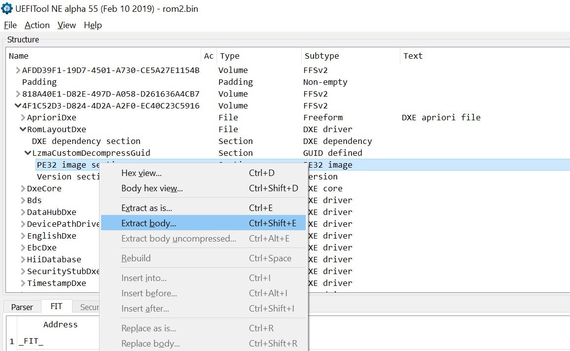
In addition to merely viewing dumped SPI flash images, UEFITool also supports extracting individual files for further analysis. In most cases, we will be interested in actual executable images which can be disassembled or debugged. To dump it, expand the desired firmware file until a section named “PE32 image section” will appear. Then, you can extract it by simply right-clicking on it and choosing “Extract body” from the drop-down menu.
Other notable candidates for unpacking UEFI firmware images include:
- UEFIExtract: This is a simple command-line utility which comes bundled with UEFITool. It supports unpacking individual files (uniquely identified by a GUID) as well as entire firmware volumes. Using this tool will generate a complete directory structure representing the firmware image, including various metadata files.
- UEFI_REtool: This is a set of Python scripts and IDA plugins which can be used (among other things) to unpack a firmware image. Unlike UEFIExtract it does not attempt to extract metadata files, but rather just the PE images.
- uefi_firmware_parser: This is more of a firmware parsing library than a full blown tool. Use it if you want to build your own tools on top of it or conduct some interactive experiments from an IPython shell.
- Ghidra-firmware-utils: This is a plugin for ghidra enabling loading of PCI Option ROMs, ROM Images, TE files (PEI modules use this stripped down version of the PE format) and include a ghidra script to name GUIDs and propagate UEFI types.
Wrapping Up
This concludes the first post of the series. Once we have unpacked the firmware image and extracted individual UEFI modules of interest, we can start analyzing, reversing and fuzzing them. To accomplish this, we will leverage some emulation tools and technologies such as Unicorn engine and the Qiling framework. These topics, alongside others, will be the main focal point of the next post.
Other Posts in Our UEFI Series
Part 2: Moving From Manual Reverse Engineering of UEFI Modules To Dynamic Emulation of UEFI Firmware
Part 3: Moving From Dynamic Emulation of UEFI Modules To Coverage-Guided Fuzzing of UEFI Firmware
Part 4: Adventures From UEFI Land: the Hunt For the S3 Boot Script